

Research
My research interests comprehend micro and nano-engineering, microelectronics, condensed matter physics and electronic transport (including: quantum new materials and high frequency solid-state devices) with a specialisation in graphene and 2D-based electronics, nanofabrication and characterization.
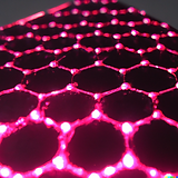
Development of 2D based heterostructures and strongly correlated materials for novel quantum electronic devices.
Since 2021 (Associate professor at JUNIA / IEMN - CNRS)
Since 2021, I have continued to work on ballistic transport within graphene microelectronic devices (as indicated below). Simultaneously, within the JUNIA/IEMN Physics of Nanostructures and Quantum Devices research group, I have applied my expertise in nanofabrication and scanning probe characterization (DC and RF) to explore the electronic properties of thin, highly correlated layers, particularly TaSe2 and NbSe2 (PhD thesis of Victor Vanduynslaeger), which exhibits current-driven phase transitions for neuromorphic applications. As the head of cleanroom training for new arrivals, I also support the activities dedicated to the study of catalytic reactions through semiconductor thin films [ACL-10] (PhD thesis of My Nghe Tran).

Graphene Dirac fermions optics and electronics
Since 2017 (Postdoctoral researcher at Ecole Normale Supérieure of Paris - CNRS)
During these four years of postdoctoral research, my focus was on studying ultra-high mobility ballistic transport phenomena in two-dimensional electron gases of monolayer graphene encapsulated in hexagonal boron nitride (hBN) heterostructures. These studies were conducted within the framework of two co-supervision PhD thesis (Holger Graef and Aurélien Schmitt) and revolved around several projects:
Firstly, my initial objective was to create graphene/hBN-based capacitors and investigate the plasmonic resonance of the two-dimensional electron gas in the high-frequency range using RF admittance. The non-classical transport properties, resulting from confinement and/or quantum coherence, manifest not only in conductance but also in RF admittance and noise. Preliminary measurements allowed us to accurately determine the dielectric properties of hBN [ACL-7]. Subsequently, we fabricated graphene field-effect capacitors and characterized them using a 70GHz network analyzer, in which we observed a plasmonic resonance at 40 GHz, corresponding to a plasmon with a wavelength of 100 µm [ACL-3]. This discovery represents a significant advancement in the realization of resonant plasmonic devices and the study of plasmons within bipolar superlattices.
We also exploited the ballistic characteristics (associated with the Klein tunneling transmission) of such devices to examine the total internal reflection of electrons. We designed corner reflectors, delineated by ultra-thin tooth-shaped gate electrodes, and demonstrated both geometric and coherent electronic optics effects [ACL-4]. In addition to demonstrating the feasibility of high-frequency Dirac fermion optics experiments, we showed that this device was sensitive to phonon scattering, opening the way for measurements of their flight time.
We also established that graphene, a semimetal, can exhibit electroluminescence under strong bias conditions. This major breakthrough in the field of light-matter interaction is demonstrated by combining various optical spectroscopy techniques and is made possible by the presence of an interband carrier injection mechanism in high-mobility, high-field graphene, the Zener effect [ALC-11].
Finally, during our efforts to push the high-frequency limits of graphene transistors, exploring the Zener interband conduction regime in particular [ACL-5], we demonstrated the existence of a mesoscopic variant linked to high-energy physics, namely the Schwinger effect, in graphene. We highlighted that a combination of the electric field enhancement effect often associated with the pinch-off regime of semiconductor transistors and the Klein tunneling effect, due to the relativistic nature of charge carriers in graphene, creates a quasi-one-dimensional transport regime that leads to Schwinger pair creation of electron-hole pairs under high-bias [ACL-8].
(PI: Bernard Plaçais - Graphene Flagship funded project)

Plasmonic and Surface-Enhanced Raman Spectroscopy (SERS)
2016-2017 (Postdoctoral researcher at CSPBAT- CNRS)
This project was focused on theoretical and experimental studies of the unique properties of gold nanostructures for the conception of new photonic and plasmonic devices. Indeed, such nanostructures, after a proper functionalization can be transformed into a bio-chip and be implemented in a specific optical instrument in order to significantly increase its performances as a biosensor. I therefore worked on the optimisation of these resonant devices in order to simultaneously enhance the Surface Plasmon Resonance imaging (SPRi) sensitivity and the Surface-Enhance Raman Spectroscopy (SERS). Gold nanostructures deposited on a thin conductive film exhibit some specific optical properties with the observation of localised surface plasmon (LSP) as well as Bragg modes where the propagating and localized modes are resonantly coupled to the array periodicity. The position of the LSP resonance peaks can be easily tuned on a large range of the visible spectrum by using these different configurations of sizes and periods of the nanodisks.
My work consisted in implementing a reliable and reproducible nanofabrication of such nanostructures in clean room by e-beam lithography with different geometrical parameters (diameters, flattening, periodicity) and metallic subfilms (ITO, Au and Al). I finally analysed each biochip by SPRi to detect and quantify in-situ the bio-targets, then by SERS to unambiguously identify the nature of these targets through their spectral signature by focusing our analysis only on the areas of interest given by the SPRi module [ACL-6].
(PI: PR. Marc Lamy de la Chapelle - NanobioSensor ANR funded project)

Thermo-mechanical Raman micro-spectroscopy
2014-2015 (Fulbright Scholar at Georgia Institute of Technology)
AlGaN/GaN semiconductor heterostructures components are expected to play a significant role in future telecommunications and power electronic systems. The major challenge lies in the significant self-heating of these GaN components, which directly affects their reliability, necessitating the development of new technologies capable of effectively managing thermal dissipation during high-power usage. Furthermore, mechanical strains in the epitaxial layers promote the presence of traps and defects in the channel, further reducing the reliability of GaN components.
The objective of this project was to investigate the fundamental factors that dictate the reliability of GaN power devices by providing essential information that can improve the technology of these components. These studies primarily focused on thermal and mechanical responses through the analysis of acoustic phonons via Raman and photoluminescent spectrometry of HEMT AlGaN/GaN structures. The study of relative deviations in the E2high and A1LO peaks, characteristic of the GaN Raman spectrum, allowed for the measurement of temperature and mechanical stress levels with micrometric spatial resolution in different GaN component technologies (HEMT, Schottky diode, PIN diode) [ACTI-7].
I also conducted significant work to improve the sensitivity of Raman measurements using semiconductor nanoparticle depositions. This technique allowed for the first-time measurement of small temperature elevations in low-power high-frequency components and direct temperature measurements on HEMT metallic gates.
(PI: Pr. Samuel Graham, Jr - Fulbright Scholar Program)

Graphene nanoribbons based high frequency electronics
2010-2014 (Thesis project at IEMN-CNRS)
The exceptional electrical and mechanical properties of graphene make this two-dimensional carbon-based material one of the flagship materials in microelectronics. The goal of this research work was to demonstrate, through the fabrication and characterization of RF components, the new possibilities offered by graphene in the field of ultra-fast and low-noise transistors.
The development and optimization of various technological processes (including the development of gate oxide by ALD, T-gate lithography, nanostructuring of the active area into graphene nanoribbons) were carried out in a cleanroom using graphene samples obtained by SiC substrate graphitization. The material's quality and properties, such as mobility, sheet resistance, and certain technological characteristics like contact resistances, were then deduced from specific measurements (AFM, Raman microscopy, Hall effect, I-V curves). Finally, electrical characterizations in both static and dynamic regime were performed on graphene field-effect transistors (GFETs) using a 67GHz network analyser. The findings revealed an interesting intrinsic current gain cut-off frequency and maximum oscillation ratio (ft intr /fmax = 82/20GHz at Vds =0.3V) [ACL-2] [ACL-1].
(PI: Pr. Henri Happy - MIGRAQUEL ANR funded project)